
Department Topper
SUGANYA N
MBA (VLSI)- I Year
CGPA
9.19

The electronics market of India alone is valued to be nearing $400 billion. Electronics and Communications is the driving force behind the growth and development of many industries
The electronics market of India alone is valued to be nearing $400 billion. Electronics and Communications is the driving force behind the growth and development of many industries
The world has become smaller thanks to electronics and communication. Just a few decades ago, it would have seemed impossible for one to communicate with someone halfway across the world in real-time, that too at an affordable price, but here we are. Today, we can, not only talk but also video chat free of cost with someone halfway across the world. We have electronics and communication engineers to be thanked for this. Electronics and communication engineering (ECE) is more of a blanket term. It actually encompasses many specializations under it like consumer electronics, analog electronics, digital electronics and more. Electronic communication engineers can be defined as engineers who research, develop and make modern-day electronic devices and communication systems. Therefore, you can judge how important this profession is.
The most important benefit that the Electronics and Communication branch provides you is the freedom to drift between hardware field and software field. Furthermore this is also the reason that a lot of industries choose to prefer Electronics and Communications engineers over other engineers. During the four years of Electronics and Communication Engineering, students gain the knowledge of both the hardware and the software aspects.
While they learn about electronic circuits, devices, and communication systems, they also learn about embedded systems, programming languages, and assembly languages. An Electronics and Communication Engineer, who has knowledge about the hardware field, and also has a grip over some computer languages, will be more successful during his career than another student who is proficient only in the software field. Hence, Electronics and Communication Engineers can switch from hardware to software field, but it is not the other way around.
The magnificence of Electronics and Communication lies in its ubiquity! Electronic devices have become a major part of our lives.
Department Topper
MBA (VLSI)- I Year
To be a department of repute for learning and research with state-of-the-art facilities to enable the students to succeed in globally competitive environment
Duration: 2 years
No. of Semesters: 4
Intake / No. of Seats: 18
Eligibility: As per the Anna University and AICTE Norms
Structure Design Engineer | Communication Engineer | HPC Design Productivity Engineer | Physical Design Engineer | VLSI HVL Verification Engineer| SoC Design Engineer| CAD Engineer | Analog Circuit/Layout Design Engineer | Synthesis Design Engineer | Verification Engineer | Testing Engineer
PO 1: Acquire in-depth knowledge of VLSI circuits and systems to discriminate, evaluate, analyze, synthesize and integrate for enhancement of knowledge
PO 2: Create, select and apply appropriate methods, systems and recent engineering and EDA tools including emulators for modeling and prototyping with an understanding of the tools limitations
PO 3: Think laterally and originally to solve various methods in VLSI circuits and related domain after considering public health and safety, cultural, societal and environmental factors in the core areas of expertise
PO 4: An ability to independently carry out research /investigation and development work to solve practical problems
PO 5: An ability to write and present a substantial technical report/document
PO 6: Students should be able to demonstrate a degree of mastery in VLSI Design. The mastery should be at a level higher than the requirements in Bachelor of Electronics and Communication Engineering
PEO 1: Analyze and solve complex VLSI circuits and systems through the acquired in-depth knowledge
PEO 2: Develop managerial skills and apply appropriate tools in the domains of VLSI design incorporating safety, sustainability and become a successful professional
PEO 3: Exhibit professionalism while communicating with local, national and foreign peers bound with regulations and leading life- long learning
PSO 1: Use EDA tools and software to design VLSI circuits and systems.
PSO 2: Integrate multiple sub-systems to develop System On Chip, optimize its performance and excel in industry sectors related to VLSI domain.
The world today runs on electronics and communications. The leaps and bounds growth we’re seeing in technology and quality of life has huge contributions from electronics and communications engineering. Therefore, there is a demand for talent in this stream of engineering. Overall, engineering is set to grow a strong 7% growth rate in the next decade. And this is just in India. There’s going to be a huge demand for engineering and electronics & communications engineers all over the world, as it constitutes a sizable portion in engineering. Electronics is the backbone of digital technology. Hence, if you’ve chosen to make a career in this stream, you are already on a path that has more likelihood of success and career growth.

























The Department of Electronics and Communication Engineering, started in 2009 and offers one UG program, PG program in VLSI Design and Full time/Part time Doctoral programs. We are accredited by NBA and recognized research centre of Anna University. We have outstanding infrastructure with 10 well established laboratories, 3 centre of excellences namely (IoT, VLSI and PCB), project laboratory, department library, seminar hall, board room and faculty cabin.
Our team comprises of experienced, energetic and dedicated faculty members with 32% PhD holders and 40% pursuing PhD. Our students bagged 12 university ranks with more than 90% results and excellent placement records providing more than 85% placements consistently from its inceptions.
| Academic Year | Name of the Faculty | Title of the Consultancy Work | Industry | Amount (In Rs.) | Status |
|---|---|---|---|---|---|
| 2019-2020 | Dr. M.G.Sumithra Dr. K.S. Tamilselvan Mr K.Siddarthraju |
Solar Panel Based VFD for Irrigation Pumps | Fulfill Electric Corporation, Coimbatore. | 98,000/- | Under Progress |
| 2019-2020 | Dr. M.G.Sumithra Dr. K.S. Tamilselvan Dr. K. Murugan |
Automatic Seed Segregation & Processing System | Surya Seeds, Dharapuram. | 72,000/- | Under Progress |
| 2019-2020 | Dr. M.G.Sumithra Dr. K.S. Tamilselvan Mr.T. Venkatesh |
IoT Based Online GSM Checker for Papers and Boards | Sri Nava Sakthe Paper Boards | 72,000/- | Under Progress |
| 2019-2020 | Dr. M.G.Sumithra Dr. K.S. Tamilselvan Mr K.Siddarthraju |
Automatic Irrigation System for Hydroponic Feeders | Wizaard Systems, Coimbatore. | 62,000/- | Under Progress |
| 2019-2020 | Dr. K.S. Tamilselvan | Design of TH Switch for E-coolers | Thumba Agro Tech, Palani. | 17,000/- | Under Progress |
| 2019-2020 | Dr.M.G.Sumithra Dr.D.Venugopal, Mr.K.Siddharthraju Mr.S.Finney Daniel |
Automation of Mask Quality Checking and Counting | Midas safety Pvt. Ltd, Coimbatore | 50,000/- | Under Progress |
| 2019-2020 | Dr.M.G.Sumithra Mr. V. Chandran |
NVDIACertified Training (Under Knowledge Sharing) | SRM University and Hindusthan University, Sanskrithi School of Engineering | 75,000/ | Completed |
| 2016 - 2017 | Dr.M.Kathirvelu Mr.B.Dinesh Mr.S.Finney Daniel |
pH Sensing Module for Drip Irrigator | Niagara Automation, Coimbatore | 6,000/- | Completed |
| 2015 - 2016 | Mr.V.P.Ajay Mr.P.Krishnamoorthy |
Rig Testing Module | Bull India Pvt.Ltd, Coimbatore | 2,14,150/- | Completed |
| 2014- 2015 | Dr.M.Kathirvelu Dr.Jaishankar Mr.B.Dinesh |
Web App Based Vehicle Tracker using GPRS | GEM Enterprises, Coimbatore | 1,50,000/- | Completed |
| 2013 - 2014 | Dr.M.Kathirvelu Dr.Jaishankar Mr.V.Govindaraj |
Wifi Based Water Level Controller | Pebbles Electronics, Coimbatore | 40,000/- | Completed |
| Total Consultancy Work Amount (Rs.) | 4,52,000/- |
| S. No. | Name of the PI/CO-PI | Title | Scheme/ Funding agency | Fund Received (Rs.) |
|---|---|---|---|---|
| 1 | Dr. Sumithra M G Dr. Seethalakshmi V Ms. Aswatha R |
Nuclear and RF radiation hazards on human beings-Control and regulatory measures | AERB | 25,000 |
| 2 | Mr. Manikandan M Student Members: Mr. Adidhyan V Mr. Gajendran M Mr. Gnana Vijay V |
Smart vehicle (Single Pedal Control) for physically challenged people using IoT voice recognition | TNSCST | 7,500 |
| 3 | Dr. Seethalakshmi V Ms. Aswatha R |
Integrative Internet of Things and Deep Learning for Smart Healthcare | AICTE | 3,58,333 |
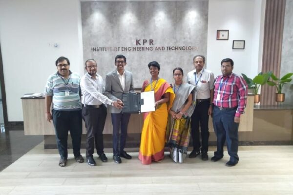
The department of Electronics and Communication Engineering has taken enormous efforts and initiatives to promote national and international academic cooperation in education. As a part of this initiative, the department has signed Memorandum of Understanding (MoU) with leading industries to collaborate in potential internship activities, setup of lab facility, technical assistance in industry sponsored projects, conducting periodic workshop/seminars, joint publications, research and consultancy for the benefit of students, faculty and research scholars of the institutes. This MoU also envisages cooperation in undertaking R & D projects in the emerging areas of technology like real time embedded systems, artificial intelligence, internet of things (IoT) and computer vision etc.
Who can study VLSI Design at KPR Institute of Engineering and Technology
A pass in a recognised Bachelor’s Degree or equivalent in the relevant field and obtained atleast 50% (45% in the case of candidates belonging to reserved category) in the qualifying degree examination
10 + 2 + AMIE (or) 10 + 3 years diploma (awarded by the State Board of Technical Education) + AMIE
Application Link Click Here
Download the strategy document to understand what are the opportunities available for a student studying ECE